CHM 678 and CHM 481 APPLIED MICROSCOPY IN RESEARCH SPRING 2017
syllabi, etc. posted 1-11-2017
syllabus chem 678 2017
syllabus chem 481 2017
example labs-anonymous
lab report format handout
Lectures and images from week 1 posted 1-11-2017
8-bit image lecture
images for lab report -trans light of mouse egg with gold labeled villi - fluorescent confocal of autofluor sandalwood callus - afm image of CdS nanowire with dna origami on top - same afm image of nanowire in original format - SEM image of spider silk - Rotary park, summer 2015
selected readings posted 1-20-2017 murphy 2nd ed
selected readings posted 1-20-2017 goldstein 3rd edition
posted 1-20-2017 digital copy of SEM lab, use diagrams straight from here for your lab report - use this to guide your report
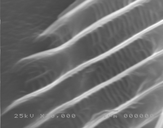
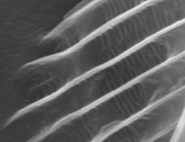
posted 1-20-2017 SEM images from first SEM lab - file names identify animals - remember this report is about SEM primarily, not flies (spot size, working distance, contrast, etc.)
posted 1-30-2017 presumed antennal scale SEM slow scan --------- fast scan
posted 2-13-2017 zipped folder with all SEM beam parameter images, depth of field instructions, and digital copy of SEM lab 2 - save to a folder right click and unzip (the EDS information and spectrum of tungsten carbide drill bit are just FYI but you could use the spectrum in lab if you want)
BELOW HERE IS ARCHIVAL - ABOVE IS ACTIVE FOR 2017
posted 2-23-2016 Norton lectures through 2-23-2016 right click and save in a folder, then unzip to same folder, tell me if there are problems
posted 3-9-2016 confocal lab handouts to assist with lab reports - confocal lab 1 - confocal lab 2
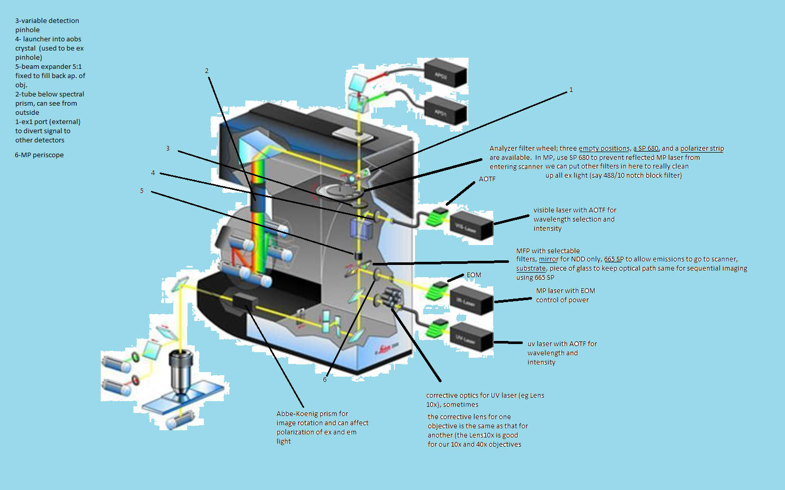
posted 3-9-2016 LeicaSP5 materials in order of importance SP5 scan head diagram - best confocal overview from Leica - quick start guide for SP5 from Leica - good Olympus LSCM intro
OLD - 2014 and before below
Lectures and images from week 1 posted 2-2016
OLD 2014 AFM lab materials for
afm lecture
mm8 -intro chapter 4
OLD, 2014 posted
lectures for weeks 1-7
AFM extras from Paul West of Agilent
OLD, 2014 SEM images for first SEM lab report posted
Reed lab supplied Silicon chips with Au microwires (made by photolithography) and Au nanowires (made by ebeam lithography)
Al sample stub for discussion of contrast and resolution